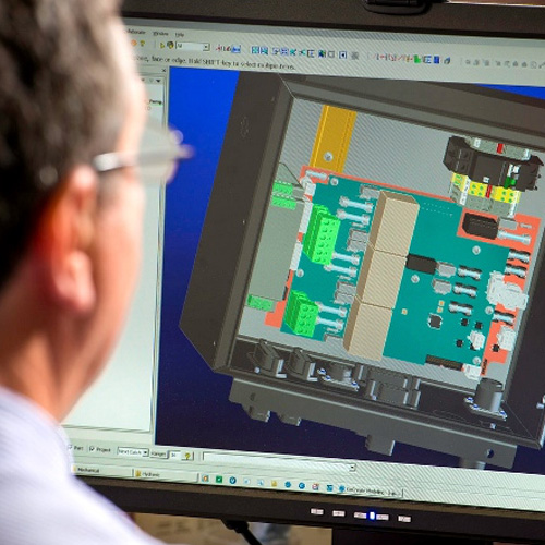
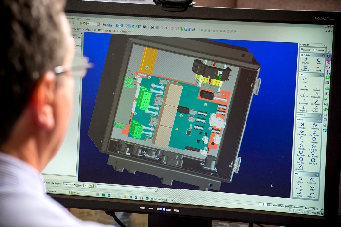
As technology continually advances, new challenges also thereby repeatedly arise for circuit board designers who aim to create products that are both economical to manufacture, and uncomplicated to test. Design for Test (DFT) is a methodology used by PCB designers, to help guide them through the sometimes very complicated PCB design and layout process – helping them ensure that the final product will be both simple and affordable to test for functionality.
Modern electronics manufacturing utilizes cost-effective methods to perform functional in-circuit tests for each printed circuit board assembly within production. Very commonly, this functionality test takes place within a ‘bed-of-nails’ style test fixture, utilizing a specially arranged array of spring-loaded probes placed in alignment to probe targets within the PCB.
As a short review of the DFT process from this previous article, three general areas are necessary to consider in order to ensure the maximum efficiency of board testability in production:
- What are the necessary electrical connections needed for a test system to perform a complete functional in-circuit test?
- What are the mechanical requirements for how to provide proper test probe access, and proper board alignment for the system?
- How does the designer then generate the appropriate data in the correct format so that a test fixture can be built by a fixture fabricator?
In this article, we will take a brief look at some of the finer details regarding how designers provide proper electrical access to each PCB by using test probes.
During the design and layout process, components known as ‘test-points’ are strategically placed by the designer on each network within the schematic, these provide access to every ‘net’ within the PCB.
Optimally, the points are mechanically defined as .035” (or larger) diameter bottom-access pads with a .1” diameter keep-away. A fixture fabricator can then easily use the resultant pick-and-place data and net-list to produce a reliable, custom fixture which uses standard probes at an affordable cost.
One key aspect of a reliable test procedure is proper probe target selection. The larger the probe target, the better the likelihood for a proper physical connection by the probes when the board is loaded into the test fixture. Targets should be as large as possible, ideally .050”-.060” when placed on the bottom of the board. Although it is more costly and difficult to test, sometimes a PCB requires top-sided probing within the test fixture. In this case, probe targets on the top side should be no smaller than .045”.
Each probe target can consist of:
- A test pad – (round or square)
- A through-hole with a soldered lead
- An open through-hole
- A non-masked via
Due to the variability in placement and edge geometry, selecting probe targets on the leads of surface mount technology (SMT) devices should be avoided. In ideal cases, industry-standard .100” spring probes are used within the fixture, which are both low-cost and reliable.
To an electronics contract manufacturer like Milwaukee Electronics, the principles of DFT are relied upon during each PCB layout and design process to create boards which are economical and uncomplicated to test.