To increase the efficiency of assembly, and detect electronics manufacturing defects, there are several considerations which designers rely on when they utilize Design for Testability (DFT) during the design and layout process of a circuit board. DFT affects how components are selected, arranged, and integrates circuit-level testability for a PCB. Its goal is to provide electronics manufacturers with a reliable, easy means by which to functionally test the workings of a fully assembled board – without requiring excessive amounts of time, cost, or labor.
The physical design of a PCB has the biggest role to play in determining how easily, or how difficult it will be for a completed unit to undergo an in-circuit test. There exist three over-arching stages for the implementation of DFT during a PCB design and layout process:
- Establish what connections on the circuit board will be necessary for an in-circuit/MDA test system from an electrical standpoint.
- Determine the mechanical requirements of board alignment, and how to provide areas for test probes to make contact with the PCB.
- Generate the appropriate data for fixture fabricators and test programmers (in an efficient format) to equip testing machinery.
For full coverage of all components and connections, a test system needs electrical access to each node (or ‘net’) on the circuit board. A node is one electrical connection on a PCB, it consists of either a pin or a lead – and is connected, (via conductors) to at least two discrete components on the board.
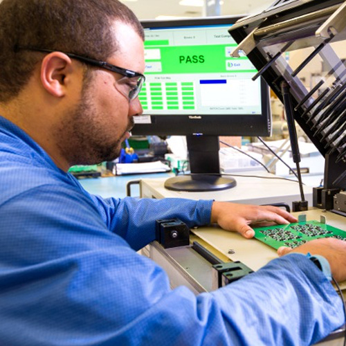
Conventional in-circuit testing equipment uses a series of carefully placed spring probes sitting inside a ‘bed of nails’ style test fixture which is uniquely paired to a single corresponding PCB unit, or a multiple-unit panel.
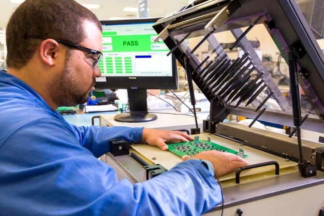
This specially-made fixture makes physical contact with the pre-selected probe targets on the PCB, which allows the test system to inspect for anomalies and defective components. DFT, and the in-circuit testing processes it supports help grant electronics manufacturers the ability to: (1) promptly catch defects after the stages of electronics assembly have been completed, and (2) rely on consistent results from their PCB assembly operations.

With regards to the specific guidelines of DFT, the following fundamental operations are used by hardware engineers during the PCB design and layout process:
- Appropriate placement, spacing, and sequencing of probe targets which provide a reliable electrical connection to each board ‘network’.
- Detailed examination of each component body size, spacing, height, and verification of visual/mechanical accessibility to all components.
- Integration of tooling holes, also known as ‘alignment holes’ – which mate with test fixture guide pins, for accurate positioning within the system.
- Adopting as compact a board size as is possible; fewer test points result in less costly testing equipment and reduction of large-board related problems (such as board-flex during vacuum fixturing).
- Optimizing the shape of the PCB; board outline shapes that are rectangular in nature are more economical to fixture.
- Restricting the number of necessary routed openings on the PCB – so minimal gasketing is required.
- Elimination of open holes (such as unmasked or unsoldered vias).
As a comprehensive set of techniques to reliably, economically, and quickly test circuit boards, DFT provides an important way for the electronics manufacturing services industry to balance the ever-increasing paces of consumer demand and product complexity.
Forthcoming blog articles will feature a continued analysis of DFT and expand upon a number of the concepts mentioned above, with greater levels of attention paid to the various electrical and mechanical considerations board designers make use of when applying it as a methodology.